 |
As we have seen, we need to make relatively large cavities. For doing that we
have to remove relatively large volumes of Si, and this we can do by either wet chemical etching or by plasma etching
- as in microelectronics. |
|
 |
However, plasma etching in microelectronics has not been engineered to remove
a lot of Si. If we would use existing processes for etching cavities, it would take forever and probably would run
out of producing the structures desired with increasing depth. |
|
 |
So let's modify those processes! Easier said than done. In fact there is one special process
for deep etching with plasma, that we will look at below, Here we must now resort to the still rather black art of wet etching. |
 |
Using isotropic chemical etchants thus as HF / HNO3 /
CH3COOH (very unhealthy!) would just produce a big hole with lateral dimensions no smaller
than twice the etching depth and some semiglobular shape. |
|
 |
Fortunately, there is such a thing as
anisotropic
chemical etching; the most prominent chemical for this is KOH
(at somewhat elevated temperatures like 80 oC. Unfortunately, alkali
metals like potassium
(K) are anathema for Si microelectronics (and thus for MEMS with some electronics integrated on the chip).
|
|
 |
The figures compare schematically isotropic and anisotropic etching. |
| |
|
 |
We cannot use KOH for the reason given above, but its anisotropic etching
properties gives us the idea to try other basic (instead of acidic) etchants. |
|
 |
What works and what we we can use is, for example, aqueous TMAH(=tetra-methyl
ammonium hydroxide; (CH3)4NOH) solutions in water (5 % - 30 % TMAHin H2O),
a harmless chemical from the viewpoint of easily-contaminated Si. |
|
 |
Often (but not always) the {111} planes act as "stop planes" for anisotropic etchants, meaning that the etching or dissolution rate on this plane
is far slower than on other planes. |
|
 |
In fact, the etching rate with these anisotropic etchants on {111} planes can be about
1 000 times smaller than on the other low-indexed planes like {100} or {110}; i.e. the selectivity is very large. |
|
 |
If you start in a square opened in some chemistry-resistant mask on typical (100) Si,
you will start to etch a perfect inverse truncated pyramid. If you etch long enough, a perfect pyramid with {111}
sides will result. as shown below - we have already seen nice examples.
|
|
 |
In the case of cantilever production as shown below, some more time would be needed to remove
the "bridges" below the larger cantilevers. A time sequence would look like this: |
| |
|
 |
Electrochemical etching
may also be highly anisotropic, but is not really used so far in mainstream MEMS technology. |
| | |
 |
Why is anisotropic (electro)chemical etching of Si a black art? There is an easy simple answer, and a more general one. The simple answer is simple: Nobody,
for example, can calculate the selectivity of the etchants named above (as a function of concentration, temperature, doping,
and so on; of course) from "first" or even second principles. |
|
Courtesy ISIT; see also "books"
|
|
|
 |
Now let's be more general: If you consider the parameter
space of an etching experiment - it is very large! You can have many compositions of the basic etchant (including
those "magical" drops of this or that); the temperature and the doping of the Si are parameters of importance.
If you actually do an electrochemical experiment, you have voltage and current as additional
parameters. The results may even depend on the state of illumination of the the Si. |
|
|
 |
Let's assume you have found a set of parameters, i.e. one "point" in this large
parameter space, that works. Now change one of the many parameters somewhat. Can you (or anybody else) predict theoretically
(i.e. without trying out, or reverting to experiments already done before) what is going to happen? The answer is: Most
likely not. Sometimes, predictions can be made with a high level of confidence, quite often unforeseen and amazing things
happen. Understanding etching of semiconductors in general therefore is still a wide open field of research |
|
 |
Nevertheless, with anisotropic chemical etching we now have a way to make cavities
in principle. This is great, but not good enough. We do not only need a large selectivity with respect to crystallographic
planes, we also need selectivity with respect to the doping of the Si. We will see why in the next sub-chapter. |
|
|
 |
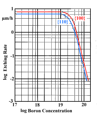
Fortunately (i.e. not predicted), for highly Boron (B) doped Si, i.e. p+-Si,
the etching rates in all direction become very small, i.e. p+-Si does not dissolve anymore in basic etchants. |
|
|
 |
The effect is quite dramatic: As soon as some minimum B-concentration [B] has
been reached, the etching rate decreases with the fourth power of [B] as shown in the figure. |
|
|
| |
| |
|
The Bosch Process |
| | |
 |
As mentioned above, the large
variety of plasma etching (also called
dry etching) process developed for microelectronics are, of course, used in MEMS
technology in many ways, but are simply not meeting all etching needs. |
| | |
| |
|
 |
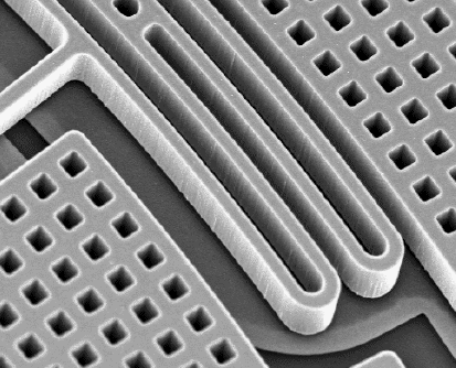
Look at the free moving part of a gyro in the picture. It consists of poly-Si
about 10 µm thick that was "etched out" of a solid poly-Si layer with very high precision.
It has all those little square holes in it for reason we will encounter later - but they need to be made. |
|
Courtesy of ISIT |
|
|
 |
The solution to many of the dry etching or plasma etching problems encountered in MEMS technology
is the high-rate plasma etching or the "Bosch
process", patented in 1994 by Bosch | |
|
 |
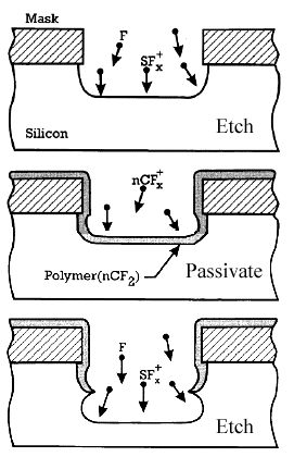
The Bosch process essentially decouples the two necessary ingredients for anisotropic etching:
1. dissolving Si at the bottom, and 2. passivating the side walls, i.e. protecting them against etching. |
|
|
| |
| |
 |
The process alternates every 10 s or so between etching Si and depositing
some polymer on the walls. The polymer deposited on the bottom of the area to be etches is taken off much faster than the
coating of the side walls, allowing some net etching into the depth at rather high speeds and for (almost) arbitrary depth. |
|
 |
The etching process uses essentially SF6 plasma chemistry. |
|
 |
Passivation uses a fluorocarbon process, using gases like C4F8
, C3F6 or CHF3. |
|
 |
Etching rates of > 10 µm/min per minute are possible, allowing cost-effective
processing even for deep etching, including all the way through a (thinned to about 300 µm) wafer. |
|
 |
The frequent switching of gases and etching parameters makes the system quite complicated
(and expensive). But the Bosch process is one of the key processes for MEMS and probably will spawn
many variants in due time. |
| |
 |

Courtesy of ISIT |
| The scalloped
shape is typical for the Bosch process. |
|
| |
|
|
Chemical Mechanical Polishing |
| | |
 |
We have encountered chemical-mechanical
polishing or CMP before - in
one sentence. |
|
 |
It is a key process for both microelectronics and MEMS. Microelectronics, however, thrived
without CMP for more than 20 years, while many MEMS products would just not be possible without CMP. |
|
 |
How is it done? In principle, it is simply grinding down the surface with an
abrasive. This is the mechanical part of polishing. The chemical
part comes in because your slurry - the liquid or viscous goo that contains fine particles of the abrasive materials, also contains chemicals that etch off only
the mechanically damaged Si. KOH, for an example, would be good at that but is not used for the reason given before. |
|
 |
The amazing (and at the time of its introduction quite unbelievable) thing is that you can
use CMP with nanometer precision on huge Si wafers - if you know all the tricks of the trade, of course. Recipes
for slurries, the kind of polishing pads to use for the kind of material you want to polish off, and everything else are
closely guarded secrets. |
| |
 |
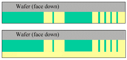 |
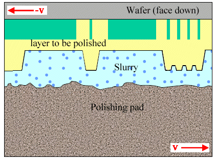
Possible results of planarization by CMPWhat you want to do is for example:
i) Just fill the
"holes" in the green layer with something "yellow",
ii) Producing a flat yellow layer on top of
the green layer (with holes filled).
Since your deposition technique produced a "rough" yellow layer, you
need CMP. |
|
 |
The figure shows the basic principle and what one can achieve. |
|
 |
CMP may also be counted to some extent among the "black arts". Not only does it have a chemical etching components; its parameter space is extremely large, too, and hard to consider in theory. |
| | |
|
Other Typical MEMS Processes |
| | |
 |
There is much more, but her we can only give a few hints. |
| | |
 |
Etching of
sacrificial layers. | |
|
|
 |
Free standing structures like in the gyro
first are made on top of some sacrificial layer that is etched off at an opportune time.
These sacrificial layers must meet a number of requirements, the most important one being that they must be compatible with
whatever is under and above it, and that there must be a way of etching them off selectively without dissolving anything
else. | |
|
 |
This is tough, man! If you just consider the etching process, it's like taking out the ham
from your sandwich without opening it up and without doing anything to the bread, butter,
mayonnaise, salad leaf etc., above and below. This means you can attack the ham only from the side, and that will take a
long time during which a lot can go wrong. | |
|
 |
One common trick is to make the top layer (the one to be free standing after the process)
full of small holes, so you can attack the sacrificial layer from more places. This is why we always see "perforated"
structures, e.g. further up. |
|
|
 |
There is no way, of course, to do the etching with plasma. You must
use "black art" chemistry. On occasion, even gases are being used (e.g. HF vapor, an extremely dangerous
chemical) because pulling filigree structures out of a liquid may make them stick together (think about your hair in the bathtub!) - even after drying. |
|
|
| |
| |
 |
Wafer bonding |
|
 |
Consider an atomically flat Si wafer with a perfectly clean (non-oxidized)
surface. Now put another wafer with an equally perfect surface on top. The two wafers would instantly bond into one piece
of Si (with a grain boundary a the interface if they were not exactly at the same orientation). |
|
 |
Real Si wafers are neither atomically flat nor perfectly clean - but they
come rather close. If you join them, they will stick together by van-der-Waals
bonding. Add a little heat and some mild pressure, and they will bond to on piece of Si. Now you have a well-established
process that was developed for microelectronics, but is not much used (too expensive). |
|
 |
In MEMS technology, wafer bonding might be a crucial process. Gyros or optical
micro mirrors operating at their resonance frequency, for example, must be kept in a cavity with a precisely established
low pressure because that determines the damping of the system. The tough part
is to keep that pressure constant for > 20 years. |
|
 |
So bond another Si wafer (with a cavity) on top. Better hermetically sealing
with no long-time stability problem at the interface is not possible, but there are many ways how to do worse. |
 |
There are many tricks to achieve efficient bonding without having to be ultra-pure
and ultra-precise. Moreover, in MEMS technology not only Si-wafer to Si-wafer bonding is used., but also,
for example Si-wafer to glass-wafer bonding. |
|
 |
This is easy to understand. Hermetically sealing your micro-mirrors with a Si
wafer on top is fine as long as you only want to work only in the infrared. If you want to use visible
light, your top better be transparent. |
|
 |
Going through the various material combinations and the technologies used to bond
them is far beyond the scope of this lecture course. Suffice it to state that bonding technologies are a major part of MEMS
processing. |
© H. Föll (Semiconductor Technology - Script)


