 |
How do we make a MEMS device? By using all processes and tricks we know from microelectronics
plus a growing number of special processes and materials developed and optimized for
one of the many MEMS products. |
 |
There are a few general processes and materials specific for most of MEMS technology
as can be appreciated by just looking at the pictures of MEMS structures already shown. In particular we often have free-standing
structures, only supported at a few points or not at all |
|
 |
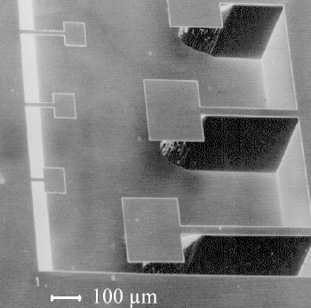
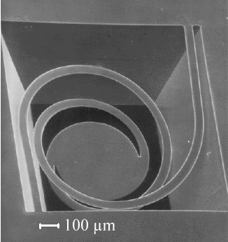
Let's look at two examples from early MEMS research to clarify this point:
|
| |

Courtesy of ISIT |

Courtesy of ISIT |
|
|
 |
- We need to be able to make deep cavities into the Si substrate.
- We need to be able to make "cantilevers" as the paradigm of a free-standing
something.
- We need to be able to make membranes.
|
|
 |
The pictures from very early (1982) MEMS R&D illustrate the
first two points quite nicely; the third point follows as a kind of corollary if you consider devices
like pressure sensors. |
|
 |
The left picture also shows one of the many problems we may encounter: There
is still some Si under the three large cantilevers - whatever etching procedure produced the cavity below the cantilevers
was not yet quite done below the larger ones. |
 |
If we contemplate these structures (and maybe this
one) again, and consider what the finished product must look like, we will also be forced to conclude the following:
- We must avoid stress in the various layers at all cost.
- We must be able to keep things absolutely planar- even on top of "topology".
- We must find special ways to hermetically seal some devices (like the gyro)
without impeding the movement of the oscillating parts; i.e. we must have special packaging
technologies.
|
|
 |
Why is it essential to avoid stress? Find out yourself!
Class Exercise:
Consider that the layer of whatever it is that forms the cantilever in the picture above would
be under tensile stress in its top part (maybe the cantilever consists of two different materials stacked on top of each
other). What would happen? |
 |
All things considered, MEMS is really a system technology. While microelectronics
can go a long way with standardized technologies, procedures and software tools, for MEMS many processes are component and
application specific, with strong interdependencies between design, electronic interfaces, system integration, packaging
and testing. |
|
 |
This means that even a very large box of tools and processes - far more than
you would need to produce any sophisticated IC - might not yet be good enough for that particular MEMS device you
are after and that means that we cannot even get close to a comprehensive survey here. |
 |
Let's finish this paragraph by considering what we do not
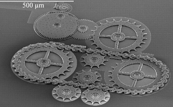
want to make: Scaled down versions of mechanical gadgets, a sort of ultra precision mechanics as shown in this picture: |
|

Courtesy of SANDIA Labs. |
|
|
 |
Pictures like that are very popular and shown a lot in "public science"
magazines. Everybody can immediately see what that is and marvel at its tiny dimensions, while a picture like the one in
the link would be received with a shrug. |
 |
But scaled down versions of gear wheels,
and so on, are rather useless. They don't work for very long, if at all, because in the micro- or nano-world, things often
behave quite differently from what would expect. |
 |
Gravitational forces, for example, become unimportant and other forces take over
(why do small dust particles not fall to the ground?). |
|
 |
Friction and surface
tension may become extremely important because the surface to volume ratio increases if things get smaller, and
forces transmitted via the surface (including friction) may dominate over forces scaling with the volume (like gravity or
inertia). |
 |
The key word now is "stiction", a newly
coined word, meaning that parts of a MEMS device that should be able to move stick to
other parts, effectively locking all movement. |
|
 |
The word also alludes to "friction" because whenever microscopic entities
slide across each other, friction, as always, does occurs - but in ways quite different from what we experience in the macroscopic
world. Friction may then lead to stiction and "dead" MEMS devices. |
|
 |
Avoiding stiction is a major concern in designing and making of MEMS structures;
more about it in the link. Generally, one should avoid sliding movements
- and that is the reason why designing device functionality by having a piece A sliding on a piece B, as in
the gear wheel picture above, is not a good idea. |
|
 |
The problem is that there is no simple way of obtaining efficient lubrication in those devices. You should now take a minute to think about the overwhelming importance of
lubrication in everyday mechanical systems like cars, and what our civilization
would look like if stiction would be a tough-to-fight macroscopic phenomena, too. |
| |
|
|
Special Materials |
| | |
 |
In terms of materials we use more or less everything microelectronics has to offer,
and then some. We have already encountered some MEMS specific materials directly or indirectly. Let's see:
- Thermal couples came up in the context of a gyro. We need
two different conductors (metals) to make one.
- The DLP chip works with mirrors. We need a highly
reflective material (= metal) for that.
- Piezoresistors came up a few times, the first time in a pressure sensor.
- Special packaging needs have appeared a few times, necessitating special materials.
- And we can be sure that there is a lot we have not yet covered.
|
|
 |
We know from microelectronics that the introduction of a new material into a
process sequence takes a lot of R&D and therefore time and money. While in microelectronics we always have "Moore's law" as a powerful economic driver,
MEMS materials are usually very application specific and progress may be slower due to economical restraints. |
 |
But lest's be clear about one thing: |
| |
Progress in MEMS technology comes from
specific Materials
and Processes |
|
|
 |
The reason for that is simple: Progress in general Si processing comes
from microelectronics - and is taken over by MEMS as soon as it become affordable. MEMS by itself could never "pay"
for, let's say, the next generation lithography technology. |
|
 |
For Materials Scientists and Engineers this are good news - you are going to
be needed! |
© H. Föll (Semiconductor Technology - Script)
