 |
After we have produced all kinds of layer, we must now proceed to the structure module of our basic process cycle. First we discuss etching techniques. |
|
 |
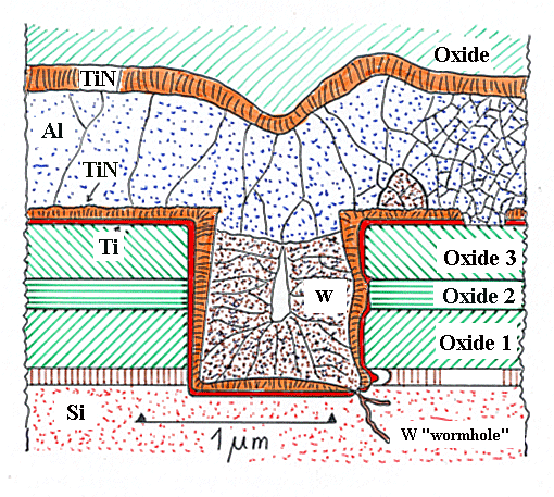
Lets see what it means to produce a structure by etching. Lets make, e.g., a
contact hole in a somewhat advanced process (and do some of the follow-up processes for clarity). |
|
 |
What the stucture contains may look like this: |
| |
|
 |
Obviously, before you deposit the Ti/TiN
diffusion barrier layer (and then the W, and so on), you must etch a hole
through 3 oxide layers and an Si3N4 - and here we don't care why we have all those layers.
(The right hand side of the picture shows a few things that can go wrong in the contact making process, but that shall not
concern us at present). |
 |
There are some obvious requirements for the etching of this contact hole that
also come up for most other etching processes. |
|
 |
1. You only want to etch straight down - not in
the lateral direction. In other words, you want strongly anisotropic etching that
only affects the bottom of the contact hole to be formed, but not the sidewalls (which are, after all, of the same material). |
|
 |
2. You want to stop as soon as you reach the Si
substrate. Ideally, whatever you do for etching will not affect Si (or whatever material you want not to be affected).
In other words, you want a large selectivity (= ratio of etch rates). |
|
 |
3. You also want reasonable etching rates (time
is money), the ability to etch through several different layers in one
process (as above), no damage of any kind (including rough surfaces) to the layer where
you stop, and sometimes extreme geometries (e.g. when you etch a trench for a capacitor:
0,8 µm in diameter and 8 µm deep) - and you want perfect homogeneity and
reproducibility all the time (e.g. all the about 200.000.000.000 trenches on one
300 mm wafer containg 256 Mbit DRAMs must be identical to the ones on the other 500
- 1000 wafers you etch today, and to the thousands
you etched before, or are going to etch in the future). |
 |
Lets face it: This is tough! There is no single
technique that meets all the requirements for all situations. |
|
 |
Structure etching thus is almost always a search for the best compromise, and new etching
techniques are introduced all the time. |
|
 |
Here we can only scratch at the surface and look at the two basic technologies in use: Chemical or wet etching and plasma or dry etching. |
© H. Föll (Semiconductor Technology - Script)
