|
Process Sequence |
| | |
 |
We start with some regular Si wafer. As far as the MEMS part is
concerned, it is just a substrate and the only requirements are that it is (extremely) flat, can be oxidized, and is process
compatible - all Si wafer meet these requirements. |
| |
|
 |
If you want to have some electronic circuitry on the same substrate, you must
now decide upon doping type and concentration, too. Here we take an n-type 1.5 Wcm
wafer. | |
|
 |
As a first process (always after cleaning etc.) we form a rather thick oxide -
2.4 µm - that serves in particular as an electrical insulation even at rather high voltages. |
|
|
 |
Obviously (??) we do that with wet oxidation. | |
 |
On top of that oxide we deposit 500 nm of poly-Si with a CVD process. It will serve as a buried conductor and therefore is called "Buried
poly". | |
| | |
| |
 |
The poly-Si needs to be highly doped if is is to be a conductor, for that
we use the old-fashioned (but simple) POCl process. |
|
|
|
 |
Ar gas is bubbled through liquid POCl3; on the hot wafer heavily
P-doped SiO2 forms that is used as a diffusion source for diffusion of P into the poly-Si. |
|
|
 |
After the diffusion the POCl-SiO2 is removed in a so-called "de-glazing"
process (wet chemistry). | |
| | |
| |
 |
In the next step the buried poly is structured (lithography
and reactive ion etching (RIE). |
|
|
 |
Then the structured buried poly is completely covered with a 1.6 µm
thick SiO2 layer, which will be the sacrificial
layer for forming free-standing structures. | |
|
 |
"Obviously" we use a TEOS
CVD process for forming this oxide - fast, low temperature and stress-free. |
|
|
| |
| |
 |
Next, the sacrificial oxide layer is structured by a 2nd lithography process,
followed by wet chemical etching for removing the exposed oxide. Since the lateral structures are rather large this is good
enough. | |
|
 |
The third lithography step follows right away, generating some openings in the
first oxide needed for contacts to the substrate. All this contacts must be below the openings in the sacrificial oxide
for obvious geometric reasons. | |
| | |
| |
 |
Now we use a first process very special for MEMS. We deposit an extremely thick layer of poly-Si - 13.6 µm. |
|
|
|
 |
In a regular CVD process this would take forever. So we do it at very high temperature
- 1 050 oC. | |
|
 |
Since normal CVD reactors are not build for this kind of process, we do it in an epitaxial reactor and call the resulting layer, somewhat self-contradictory,
"Epi-poly". The expression "epi-poly " is
certainly a fine oxymoron but you better get used to things like that. |
|
| |
| |
| |
 |
The epi-poly layer is rather rough, so we now use CMP (chemical -mechanical
polishing), one of the processes we had listed as quite MEMS specific, to make it perfectly flat. |
|
|
|
 |
The epi-poly will contain some mechanical stress - you just can't make a rather thick layer
quickly without building up some stress. So we anneal everything ("stress anneal"), for somewhat obscure reasons
in an oxygen atmosphere. | |
|
 |
Since we will then oxidize some of the epi-poly, this oxide needs to be removed in another
wet-chemical process step. | |
| | |
| |
|
 |
Now it is time to produce the first metal layer; we take Al in this case. |
|
|
|
 |
It is deposited by sputtering 1.3 µm on Al on top of the epi-poly followed
by the 4th lithography and wet chemical structuring., |
|
|
| |
| |
 |
At this point we need to use another MEMS specific process: the Bosch process or deep plasma etching.
We need to structure the very thick epi-poly layer, and standard microelectronic processes just can't do this. |
|
|
|
 |
A fifth lithography defines the structures, and the alternating etching -side wall passivation
process digs deeply into the layers, possibly creating some steps at interfaces |
|
|
| |
| |
 |
A last very typical MEMS process follows: Removal of the sacrificial oxide by
HF gas etching. | |
|
|
 |
This is a process we would never use in microelectronics - far too messy and extremely dangerous!
So why do we do it? | |
|
 |
Think about what happens when you wash your hair and withdraw this long flexible fine structures
from the liquid water - they stick together because of capillary forces.
| |
|
 |
Exactly the same thing happens when you withdraw the flexible fine structures released after
dissolving the sacrificial oxide in some liquid - they stick together.
But in contrast to your hair they will never ever come apart again - stiction
takes over. | |
|
 |
No capillary forces if you etch with gas - but lots of other problems that need to be solved. |
|
| |
| |
|
 |
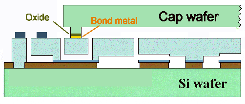
All that remains to be done is to seal the gyro hermetically at a defined pressure
that will not change in the next 20 years or so. | |
|
|
 |
For this we bond a pre-structured
Si wafer with some bond layers over the sensitive part, leaving the electrical connections free. We now have used
thelast MEMS specific process: Wafer Bonding.
|
|
|
 |
The total encapsulation process is a whole process sequence in its own right, but here we
leave it at that.. | |
| |
| |
 |
Now we have a functioning gyro. If it works to specification, you now can sell
it - for a few € a piece, if you are lucky. |
© H. Föll (Semiconductor Technology - Script)

