 |
Plasma etching, also known as dry etching (in contrast to wet etching) is the universal tool for
structure etching since about 1985. In contrast to all other techniques around chip manufacture, which existed in
some form or other before the advent of microelectronics, plasma etching was practically
unknown before 1980 and outside the microelectronic community. |
|
 |
What is Plasma etching? In the most simple way of looking at it, you just replace
a liquid etchant by a plasma. The basic set-up is not unlike sputtering, where you not only deposit a layer, but etch the target at the same time. |
|
 |
So what you have to do is to somehow produce a plasma of the right kind between some electrode
and the wafer to be etched. If all parameters are right, your wafer might get etched the way you want it to happen. |
 |
If we naively compare chemical etching and plasma etching for the same materials
to be etched - lets take SiO2 - we note major differences: |
|
| Chemical
etching of SiO2 |
Plasma etching
of SiO2 |
| Etchant:
HF + H2O (for etching SiO2. |
Gases:
CF4 + H2 (or almost any other gas containing F). |
| Species in solution:: F–,
HF–, H+SiO42–, SiF4, O2
- whatever chemical reactions and dissociation produces. |
Species in plasma and on wafer:
CFx+ (x £ 3), and all kinds of unstable species not existent
in wet chemistry.
Carbon based polymers, produced in the plasma which may be deposited on parts of the wafer.
|
| Basic processes:
SiO2 dissolves |
Etching of SiO2, formation of polymers, deposition of polymers
(and other stuff) and etching of the deposited stuff, occurs simultaneously |
| Driving force for reactions: Only "chemistry",
i.e. reaction enthalpies or chemical potentials of the possible reactions; essentially equilibrium thermodynamics |
Driving force for reactions: "Chemistry",
i.e. reaction enthalpies or chemical potentials of the possible reactions, including the ones never observed for wet chemistry,
near equilibrium,
and non-equilibrium physical processes", i.e. mechanical ablation of atoms by ions
with high energies. |
| Energy for kinetics: Thermal energy only,
i.e. in the 1 eV range |
Energy for kinetics: Thermal energy, but also
kinetic energy of ions obtained in an electrical field. High energies (several eV to hundreds of eV) are possible. |
| Anisotropy: None; except some possible {hkl}
dependence of the etch rate in crystals. |
Anisotropy: Two major mechanisms
1. Ions may have a preferred direction of incidence on the wafer.
2. Sidewalls may become protected through preferred deposition of e.g. polymers
Completely isotropic etching
is also possible |
| Selectivity: Often extremely good |
Selectivity: Good for the chemical component,
rather bad for the physical component of the etching mechanism. Total effect is open to optimization. |
|
| |
| |
 |
If that looks complicated, if not utterly confusing - that's because it is (and
you thought just chemistry by itself is bad enough). | |
|
|
 |
Plasma etching still has a strong black art component, even so a lot of sound
knowledge has been accumulated during the last 20 years. |
|
|
 |
It exists in countless variants, even for just one material.
| |
|
 |
The many degrees of freedom (all kind of gases, pressure and gas flux, plasma production,
energy spread of the ions, ...), or more prosaically, the many buttons that you can turn, make process development tedious
on the one hand, but allow optimization on the other hand. | |
 |
The two perhaps most essential parameters are: 1. the relative strength
of chemical to physical etching, and 2. the deposition of polymers or other layers on the wafer, preferably on the
sidewalls for protection against lateral etching. | |
|
 |
The physical part provides the absolutely necessary anisotropy, but lacks selectivity |
|
|
 |
The chemical part provides selectivity. |
|
 |
Polymer deposition, while tricky, is often the key to optimized processes. In
our example of SiO2 etching, a general finding is: |
|
|
 |
Si and SiO2 is etched in this process, but with different etch rates
that can be optimized | |
|
 |
The (chemical) etching reaction is always triggered by an energetic ion hitting the substrate
(this provides for good anisotropy). | |
|
 |
The tendency to polymer formation scales with the ratio of F/H in the plasma. The etching
rate increases with increasing F concentration; the polymerization rate with increasing H concentration. |
|
|
 |
Best selectivity is obtained in the border region between etching and polymer formation. This
will lead to polymer formation (and then protecting the surface) with Si, while SiO2 is still etched.
The weaker tendency to polymer formation while etching SiO2 is due to the oxygen being liberated during
SiO2 etching which oxidizes carbon to CO2 and thus partially removes the necessary atoms
for polymerization | |
 |
Enough about plasma etching. You get the idea. |
|
|
 |
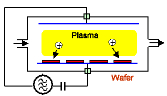
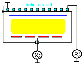
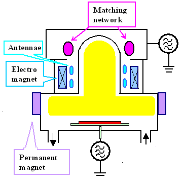
The thee pictures show extremely schematically different set-ups of plasma etchers. Essentially
the big deal is how the plasma is made. For sufficiently large etching rates, you want a dense homogenous plasma with control
of the ion energy. | |
|
 |
A taste treat of what it really implies
and some explanations to the pictures can be found in the advanced module in the link |
|
© H. Föll (Semiconductor Technology - Script)


