|
5.3.3 Stacking Faults |
 |
In chapter 4.2.1
we generated simple crystals (with just one atom per lattice point) by stacking spheres in exactly the way you would do
when you put up a mound of oranges or cannon balls. You start by arranging the spheres on a plane as densely as you can.
Than you start the second or B layer on top of the first or A layer. Naturally you put the spheres of the
second layers in the hollows or dents of the first layer. |
|
 |
When you go for the third layer you have a choice. You can go for the option where the spheres
of the third layer are in those hollows of the second layer that the third layer sits right on top of the first layer and
thus is an A layer again.
Or you go for the other option where you produce a C- layer. We found that two kinds of stacking sequences both lead to a close-packed
crystal:
- The stacking sequence ABABABA... produces an hexagonal crystal (hcp; hexagonal close packed)
- The stacking sequence ABCABCA... produces a cubic face-centered fcc crystal.
|
 |
Before we looked at all this stacking stuff from the top. Now let's restrict ourselves
to the fcc lattice / crystal and look at it sideways. Here is what you would see (schematically, of course!) |
| |
 |
| Perfect and faulted stacking sequence for an fcc crystal |
|
 |
On the left-hand side we look at a perfect fcc crystal. The A-layers are
on top of the C -layers, the B-layers..., and so on. Rather boring. |
|
 |
Now look at the right-hand side. A devious person has put an A-layer on top of a B-layer
and thus broken the monotony by creating a planar defect that is aptly called: stacking fault.
Well, why shouldn't one do this? If you look at the contraption from
the top the proper C-layer or the faulty A layer look pretty much the same. Stacking faults thus should
occur all the time? |
|
 |
Well - no! At least not for the reasons you may have in mind. Atoms "in"
a stacking fault do see an environment different from atoms in the perfect bulk, in particular if they look beyond just
their nearest neighbors. That means they have not the best possible environment and this are not in a nirvana state.
In other words, a stacking fault has some stacking fault energy (per area unit)
just like grain boundaries and phase boundaries. Nirvana will not be attained if stacking faults are around, just as nirvana will
not be attained with grain boundaries around. |
 |
So why are we doing this? Because stacking faults are very important
defects, in particular in fcc and hex crystal. And where are they coming from? |
|
 |
Good question! One might assume that they simply are formed when the material
is formed and that they cannot be "taken out" again later - just like grain boundaries. That is true enough in
some cases but the full truth is more complex: |
| |
|
Stacking faults occur:
|
1. during crystal growth,
2. as part of other defects
3. because they evolve from other defects
|
|
 |
Three reasons for stacking faults. Let's look at them one by one: |
 |
1. Stacking faults
occur during crystal growth |
|
 |
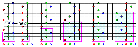
Just one example: Silicon carbide (SiC),
an extremely interesting material for electronics, comes in many different types of lattices. The figure below shows just
six. It is is obvious that about any stacking sequence can exist. It is just as obvious that you can have any number of
stacking faults in there too. |
| |
 |
| Six different silicon carbide (SiC) crystal structures (or polytypes) |
|
|
 |
Here is the reason why you (most likely) don't have silicon carbide electronic
components in your possession. It is just too damn difficult (and expensive) to make a perfect crystal as needed for electronic
applications. |
|
 |
You also need to be careful not to produce stacking faults when making silicon
or other important crystals while the material solidifies. It is not too difficult, however, to avoid stacking faults in
these cases so nothing more shall be said about this point. |
 |
2. Stacking faults are part of other defects |
|
 |
If I would have already introduced the one-dimensional
defects called dislocation, and if, in discussing that defect, I would go all the way
to what is called "partial dislocations" and "split dislocations", I now could
enlighten you about stacking faults being an integral part of dislocations, interfering mightily with their properties. |
|
 |
I didn't and I won't - so forget it. All that stuff is very important for intimately
understanding materials - but way beyond what I'm dealing with here. Consult the dislocation
science module if you want a taste treat. |
 |
3. Stacking faults evolve from other defects
|
|
 |
Now that is easy. Imagine a crystal at high temperatures. It will be full of
vacancies because that is part of nirvana. In the schematics I have adopted here, it looks like the upper half of the figure
below.
Now crank down the temperature. The point defect concentration needed for nirvana decreases
sharply. But how? Where do the surplus vacancies or self-interstitials go? Well - to the grain
boundaries as we just asserted! Absolutely true. That's what they do in normal fine-grained poly crystals.
But how
about single crystals or crystals with large grains, where the grain boundaries are
far, far away? |
|
 |
In this case vacancies (and self-interstitials, if around) tend
to agglomerate or cluster, often in a small disc. This is shown below on the right-hand side for vacancies.
The rest
is obvious. If the vacancy disc gets large enough, the two "surfaces" just collapse and bond to each other, forming
a stacking fault disc in the process as shown on the left hand side. |
| |
 |
| How stacking faults evolve from vacancy agglomeration. |
|
 |
This is quite serious if you are into defect-free crystals like silicon or all
the other ones needed for all kinds of microchips. |
|
 |
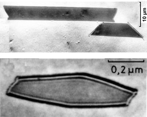
The electron microscope pictures below show stacking faults formed by agglomerating
silicon self-interstitials. Forming a layer of atoms squeezed in between the regular
layers is their only way of escape; this
link provides a picture. The vacancies, while also agglomerating into stacking fault discs as shown above if they feel
like it, have an alternative: they could also form a three-dimensional hole or void. |
| |
 | | Stacking faults as seen in an electron microscope. |
|
|
 |
This is a projection of an inclined plane - the stacking fault plane - onto the
screen. The upper picture shows two rather huge stacking faults produced during processing silicon. The lower picture shows
a small hexagonal stacking fault loop produced during crystal growth. The "zebra" pattern is a result of the inclination.
Stacking faults in silicon like the ones above kill an electronic device, so they are much feared and investigated.
They wouldn't do much to a steel sword, however, so I'm not going on about this - except to make one major point:
You
have just witnessed how small zero-dimensional point defect can generate a huge two - dimensional defect. It is just one example for relations between defects. The rule is: |
| | |
All defects interact and are somehow connected
|
|
© H. Föll (Iron, Steel and Swords script)


