 |
In the beginning of a thin layer we have a substrate with a "receptive"
surface (being pretty clean at the minimum) and a source of atoms or molecules that are supposed to build up on the substrate. |
 |
How do we build up a thin layer? Let's do it in a very simple manner. We put on
our good glasses, the ones that allow us to see atoms. (Hint: you don't see with your
eyes, you actually see with your brain. Eyes are just one source of input to the seeing
center of the brain). Moreover, we do the most perfect experiment we can imagine, because here we will work with perfect
materials in a perfect world - in our minds, where this is easy. |
|
 |
So we have a perfect substrate crystal with a perfect surface - no oxide on it,
no other dirt, no whatever Also no surface
reconstruction (if you want to find out what that means - activate this link).
But perfect, in the sense of minimum free enthalpy,
still entails some vacancies even in thermal equilibrium; being of a gentle disposition we also allow mild deviations from
perfection as required by thermal equilibrium and allow a few surface steps and the occasional dislocation. |
|
 |
From some unnamed source we produce a constant stream of atoms (or molecules)
that are supposed to form our thin film on the substrate. They have some average velocity and move more or less in the direction
of the substrate. |
 |
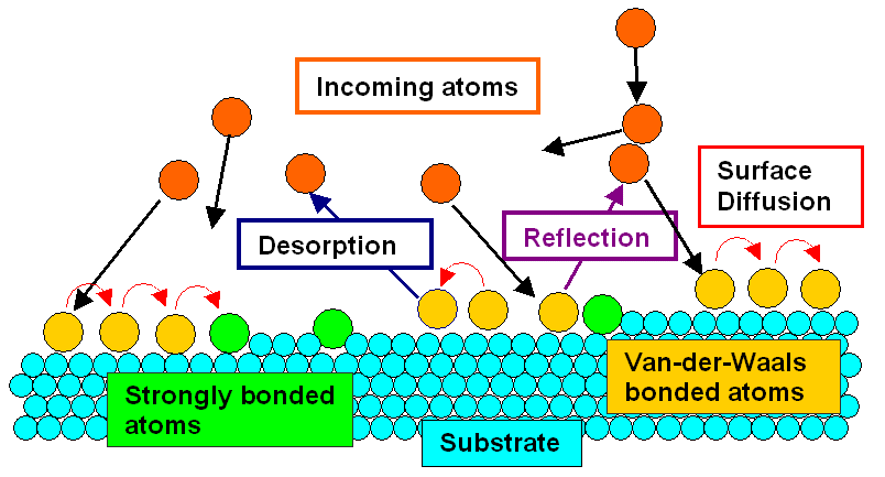
What happens when an incoming atom hits the surface of the substrate? Well, just
about anything you care to imagine: |
|
|
- The atom may just be reflected like at solid wall and then runs away to infinity.
- The atom may just be reflected like at solid wall but then hits an incoming atom and is redirected to the substrate.
- The atom may loosely bond to one or two of the substrate atoms (by one or the other of the secondary
bonding mechanisms, like "van der Waals"), or, to use surface
science terminology, it will become "physisorbed".
- At finite temperatures, it may now jump to equivalent positions in its neighborhood, i.e. it diffuses
in a 2-dimensional random walk manner on the
surface.
- On occasion, while running around at random, it may just get desorbed again and flies
off into the wide world out there.
- But then it may also find a cozy place where it can seriously bond to more than
just one (or two) substrate atoms, it will get chemisorbed; i.e. bonded by one of the
strong bonding mechanisms.
- This chemisorption will happen with higher probability if our so far loosely bonded
or physisorbed atom is seriously cornered by the substrate atoms - at a step or a surface
vacancy, for example
|
|
|
|
 |
It's all in the picture, and all of that (and more) is really happening. |
|
 |
Atoms, as the saying goes, are only human after all (or was it: humans are only
atoms, after all?). They fool around if they can, and only get seriously stuck if they fall into "traps", or to
put it more positively, if they find highly attractive situations. |
 |
All in all, we can draw two major conclusions from this simple picture: |
| |
- Not all atoms reaching the substrate "get stuck". The percentage of "B" atoms (or molecules)
remaining on the substrate A (the sticking coefficient") depends on
many things, but the probably most important parameter is the binding energy between A and B.
- In the initial phase of layer growth - the nucleation phase - first clusters
of B atoms (or molecules) most likely form at irregularities of the substrate, in particular at (atomic) steps.
|
 |
The question coming up now is how many steps (per cm2) we might
have on a given substrate and how we can optimize the step density if that is what it takes. |
|
 |
This is easy to answer on a first glance. You can even take off your sharp glasses
and just imagine a perfect
{100} or {111} oriented surface of a fcc crystal, for example. There will be no steps. But look at
the picture above. Steps in regular intervals are an unavoidable consequence of a substrate simply orientation that is off
a bit from - in the picture - precise {110}. |
|
 |
If d111 is the distance between {111} lattice
planes, and dstep is the average distance between steps like in the picture above, the misorientation a is simply given by |
| |
|
|
 |
At this point, we get a first idea why semiconductor companies making Si
chips order their wafers on occasion with a specification like "2o off {100}". |
 |
Not so easy perhaps, on a second glance, is to imagine that even surfaces with
no misorientation from, for example, {100}, might still have a certain density of steps.
|
|
 |
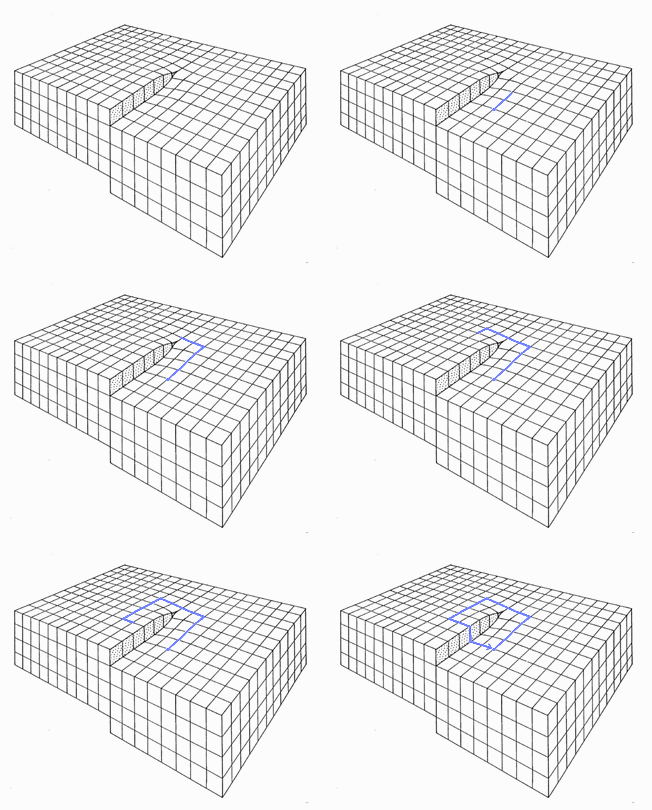
This step density, to give you a hint, is identical to the density of screw dislocations terminating at that surface. Below is an picture
of a screw dislocation ending at a surface; a Burgers
circuit running around it shows that the Burgers vector is parallel indeed to the dislocations line direction. |
| |
|
 |
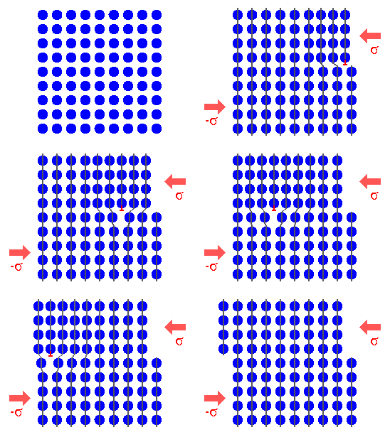
If you now recall that edge dislocations
that left the crystal, automatically produced a step
in the surface, you finally get the picture: |
|
 |
If your substrate contains defects - dislocations, grain boundaries, and so on, you might
have steps even for a perfect low index surface orientation. |
 |
What happens in the beginning of a deposition process where some atoms (or molecules)
are brought in contact with a substrate surface, thus depends on many parameters. All the processes that take place in parallel,
and with some possible interaction, may produce an exceedingly complicated situation. Mind, its complicated - but not difficult. |
|
During Growth
|
| |
|
 |
This module is not really the right place to discuss what happens
during the growth of a layer, but this topic fits here very nicely with what has been described so far.
|
 |
We simply ask ourselves: How does the general situation change after
we - somehow - have already produced a thin layer of B and, keeping the process running, now just make it thicker? |
 |
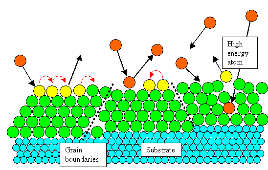
The answer is. Not much changes. Look at the picture below: |
| |
|
|
 |
It's pretty much the same as the picture form above, For varieties sake one more
process has been added: A relatively energetic B atoms hits the B-layer so hard that it penetrates into the
layer, causing some damage, and kicking one (or more) already physisorped B-atom out again. |
|
 |
It is also quite clear that you will produce grain boundaries and other defects
in the B-layer because things - atom size, lattice constants, lattice types - just don't match. |
|
 |
Of course, sticking coefficients and all
other numbers you can attach to the atomic processes might be quite different in the "B hits B"
case in comparison to the "B hits A" case. |
|
|
|
How Do We Know
|
| |
|
 |
It's easy (and amazingly cheap) to look at what is going during thin
film growth at atomic dimensions with your good glasses, the ones that allow you to see atoms. But how do we know
that what we "see" is the truth? |
|
 |
Your choices are limited. If you are convinced that what you "see"
is the truth, but you cannot corroborate your finding with independent evidence, you must either found a new religion or
become a philosopher. |
|
 |
If you prefer to remain a scientist or engineer, you now must find some way to
prove in a mathematical sense that what we discussed so far is the truth. Well - Good Luck to you! |
 |
It's generally not so easy to really see on
an atomic scale, and to make things worse, you want to see a dynamic process, where things change rapidly. |
|
 |
This is just not possible with the usual tool, the High-Resolution
Transmission Electron Microscope (HRTEM) - it just can't give "surface dynamics".
|
|
 |
The big boost to this topic came with the invention of the Scanning Tunneling Microscope (STM)
in 1980 by Gerd Binnig and Heinrich Rohrer (Nobel prize 1986) and the whole family of "Needle scrapers"
following, in particular the Atomic Force Microscope (AFM). Before that, one
could draw pictures like the ones here easily, but back in the Lab it was guess work. |
 |
We will come back to these instruments, but already now you can appreciate how
important the invention and development of these instruments was to the thin film communities (and others). |
|
 |
Finally, you may enjoy to look at some spectacular pictures produced by these instruments in the link to the company Omicron. A few selected
examples are also found in this (future) advanced module. |
© H. Föll (Semiconductor Technology - Script)


