 |
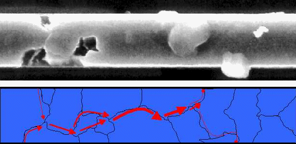
| The picture below shows an Al circuit line of an IC; it is about 1 µm across. | |||
| It has been "stressed" for some time by running a DC current through it at temperatures and current densities somewhat higher than what it would encounter in normal operation. The minus pole was on the left. The current density may have been in the105 A/cm2 region. | |||
| This is a hell of a current density - several orders of magnitude larger than what you would feel comfortable with in normal wires. | |||
| The conductor line obviously has suffered from this treatment. In its left part - close to the minus pole - holes or pits have formed, and in its right part - close to the plus pole - we have extrusions or hillocks. | |||
| Obviously, substantial amounts of Al have migrated to the right: leaving back holes and generation hillocks. and | |||
| Considering that a huge number of electrons was driven from left to tight by the current source, it almost looks as if those electrons have pushed some Al-atoms along. | |||
| This is indeed what has happened. The phenomena of electromigration is, in general terms, a drift in the diffusion currents induced by the "electron wind" | |||
| Remember that there is always some self-diffusion, but without any driving forces, the net diffusion current in one direction is always cancelled by the exact opposite current in the other direction. | |||
| Exactly how those electrons push atoms about, is still a bit obscure, but the effect is clearly there, and appreciable in finite time spans if the current densities are extremely large. | |||
| |||
| You thus would expect that electromigration scales with the self-diffusion coefficient, and thus is more severe in materials with a low melting point. | |||
| Yes, but classical self-diffusion is a bulk property. In our poly-crystalline Al, we also have diffusion along grain boundaries, which is generally much faster than bulk diffusion. | |||
| A more detailed analysis of the picture above (which, incidentally, are from the thesis work of Dipl.-Ing. Wedemeyer in 1998) that includes the grain boundaries clearly demonstrates that grain boundaries indeed provide the main pathway for the movement of the Al atoms. | |||
| At the holes, the cross-section of the Al wire is reduced, i.e. its local resistance R is larger, and the locally dissipated power L = I2 · Rat a constant current I goes up. | |||
| The wire heats up at the holes, electromigration becomes more severe, holes get bigger, and soon you have a complete interruption of the current path and thus the end of your IC. | |||
| We have a problem. As dimensions shrink by a factor of k, the cross-sectional area of the Al lines tends to shrink by k2, but the current only goes down linearly with k. | |||
| With shrinking dimensions current densities thus tend to go up, and electromigration in pure Al (or Al with some Si to prevent spiking) would have made integrated circuits with a life time of 10 years simply impossible in the 80ties of the last century. | |||
| You must do something. Avoiding grain boundaries roughly parallel to the wire helps, but how are going to do this? Well, there are some tricks which help to create the "bamboo structure" you want, but this would not be sufficient. | |||
| So you do what you always do in this kind of situation: You add some dirt to your Al and hope for the best. | |||
| Maybe, the right element "poisons" the grain boundaries, making grain boundary diffusion for Al atoms more difficult. Or maybe..... | |||
| Having a "theory" or just a hunch to work from helps; but not too much. Doing is what really helps. And yes, if you add about 0.5 % of Cu, electromigration becomes less severe. This is also true for other elements, but Cu is what is mostly used. | |||
| However, if only a tiny fraction of that Cu ever diffuse into the Si, it will kill your device. Also, your etching process for Al may suddenly not work anymore. And your Al metallization now might be more sensitive to corrosion. And the adhesion of the next layer is now different . And.... | |||
| You get the drift: There will always be a lot of demanding work out there for highly qualified people like you! | |||
![]() 6.4.1 Physical Processes for Layer Deposition
6.4.1 Physical Processes for Layer Deposition
![]() Spiking and Epitaxial Si in Contact Holes
Spiking and Epitaxial Si in Contact Holes
© H. Föll (Electronic Materials - Script)