 |
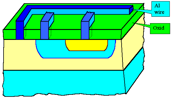
So all you do is to cover everything with an insulator. For that you are going
to use SiO2, which is not only one of the best insulators there is, but is easily produced and fully compatible
with Si. |
|
 |
On top of this oxide you now run your "wires" from here to there, and wherever you
want to make a contact to a transistor, you make a contact hole in the SiO2
layer. |
|
 |
Every transistor needs three contact holes - and as you can see in the drawing, you rather
quickly run into the problem of crossing connections. |
 |
What we need is a multi-level metallization,
and how to do this is one of the bigger challenges in integration technology. |
|
 |
Fortunately, we already have a second level in the Si - it is the "buried
layer" that we put down before adding the epitaxial layer. It can be structured to connect the collectors of
all transistors where this makes sense. And since the collectors are often simply connected to the power supply, this makes
sense for most of the transistors. |
|
 |
But this is not good enough. We still need more metallization layers on top. So we repeat the "putting
oxide down, making contact holes, ..etc". procedure and produce an second metallization layer: |
| |
|
 |
If you get the idea that this is becoming a trifle complicated, you get the right
idea. And you haven't seen anything yet! |
|
 |
State-of-the-art ICs may contain 7 or more connection (or metallization) layers.
For tricky reasons explained later, besides Aluminium (Al), Tungsten (W) is employed, too, and lately Al
is being replaced by Copper (Cu). |
|
 |
Between the metal layers we obviously need an "intermetal
dielectric". We could (and do) use SiO2; but for modern chips we would rather use something
better. In particular, a material with a smaller dielectric constant (SiO2 has a value of about 3.7).
Polymers would be fine, in particular polyimides, a polymer class that can "take the heat", i.e. survives at relatively
high temperatures. Why we do not have polyimides in use just now is an interesting
story that can serve as a prime example of what it means to introduce a new material into an existing product. |
 |
Why are we doing this - replacing trusty old Al by tricky new Cu
- at considerable costs running in the billion $ range? |
|
 |
Because the total resistance R of an Al line is determined by the specific
resistivity r = 2,7 µWcm of Al and the geometry
of the line. Since the dimensions are always as small as you can make it, you are stuck with r. |
|
 |
Between neighbouring lines, you have a parasitic capacitance C, which again
is determined by the geometry and the dielectric constant e of the insulator between the
lines. Together, a time constant
R · C results, which is directly proportional to r · e.
This time constant of the wiring - found to be in the ps region - gives an absolute upper limit for signal propagation.
If you don't see the probem right away, turn to this basic module. |
|
 |
In other words: Signal delay in Al metallization layers insulated by SiO2
restricts the operating frequency of an IC to about 1 GHz or so. |
 |
This was no problem before 1998 or so, because the transistors were far slower anyway.
But it is a problem now (2000 +)! |
|
 |
Obviously, we must use materials with lower r and e values. Choices are limited, however - Cu (r = 1,7 µWcm) is one option that has been chosen; the last word about a suitable replacement for SiO2
(having e = 3,7) is not yet in. |
 |
Here are famous pictures of an advanced IBM chip with 7 metallization layers,
completely done in W and Cu. In the picture on the left, the dielectric between the metals has been etched
off, so only the metal layers remain. |
| |
|
© H. Föll (Semiconductor Technology - Script)
