 |
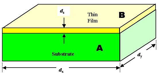
That is fine, but now let's look at some thin films with a more involved geometry or topology as the case might be: |
| |
| |
|
In the first picture we have a more realistic situation, The surface
of the substrate A, onto which we deposit our thin film B is rough.
This is certainly realistic, because complete absence of roughness would mean atomically flat, which is not impossible but
hard to imagine in a real world. | |
|
|
 |
Note that the roughness of the interface and the roughness of the thin layer surface may be
correlated (as drawn), but this must not necessarily be so. The link
provides an example for NiSi2 (thin) layers on a Si substrate where the interface roughness and
the surface roughness is quite different. | |
|
 |
Two questions come to mind - How do we define and measure roughness?
- How rough will it be in typical situations?
|
|
|
 |
You know the answer to the first question from your Lab
classes: | |
|
 |
Measure the deviations zi at regular intervals i from
an ideally flat average surface (dotted line in the drawing; note that you may have two surfaces or interfaces with different
roughness) and take the "root mean square" (RMS) for the roughness R, i.e. |
|
|
| |
|
|
|
| R | = | æ
ç
è
| 1
N | |
N
S
i=1 | zi2 |
ö
÷
ø | ½ |
|
| |
|
| |
|
|
 |
Usually you can't do that, so you measure from an arbitrary ideal surface somewhere,.
Then simply subtract the average, i.e. use (zi – <zi>)2 in the sum. Simplified, we might also use an average
roughness Ra according to |
|
|
| |
|
|
|
| |
|
| |
|
|
 |
What kind of roughness do we find (or want) in typical situations? There is a clear and simple
answer: It depends! We will look at that whenever we encounter it in semiconductor technology. |
|
|
 |
By the way, the RMS of the roughness may be much larger than the thickness of the thin
film. The second picture shows just that - and it would be a good illustration for certain solar cells where dz
would even be considerably smaller! | |
 |
The third picture shows a case where there is some interface roughness, but the
surface is quite smooth. | |
|
 |
Well - why not? Realistically, however, the surface is quite smooth because you made it so
- by a special process called "chemical mechanical polishing" (CMP). |
|
|
 |
Actually, what we see here in a highly stylized form is the key process
for integrated circuits after, let's say, 1995. If you look at the picture of the IBM chip shown before, you could see exactly that: A thin layer of oxide was deposited on
a rough substrate (with Cu wires on it), but the surface at the oxide is perfectly flat. |
|
 |
The last picture show some aspects of thin films in semiconductor technology. |
|
|
 |
Our thin film may be flat on top but accommodating "roughness" in the substrate
(on the left), conformally following the substrate (and then completely cover "little"
holes; on the right), and it may be structured, i.e. having defined "holes". |
|
|
| |
 |
All in all, just defining, describing and measuring "geometry" and "topology"
(and ignoring exactly what the difference is between those two terms) can be a demanding task. |
|
 |
However, we will not waste time and brainpower to delve into this topic more deeply
but will tackle it whenever it comes up in semiconductor technology. |
| | |
|
© H. Föll (Semiconductor Technology - Script)
