 |
A case could be made that passivation of surfaces (for the early bipolar devices)
and of the Si/SiO2 interface in MOS technology, was the key process
in the beginning of semiconductor technology. |
|
 |
The reason was that early devices simply did not work - the electrical function of properly
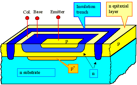
made pn-junctions and so on was overwhelmed by the surface states. To understand that, consider that every pn-
junction in a real device will come out at the surfaces somewhere: |
|
|
|
|
 |
The picture shows a typical bipolar transistor in an integrated circuit (from around 1990),
and you see a lot of pn-junctions coming out at the surface. |
|
 |
The solution was simple (but took a while to find): in the old days it consisted of simply
oxidizing the whole device; taking advantage of the low interface state density in a Si/SiO2 interface
obtainable with a "good" thermal oxide. |
 |
Modern solar cells, just consisting of the yellow and light blue layer in the schematic drawing
above, still have this problem: The pn-junction comes out at the side, with all kinds of problems. |
|
 |
The good old oxidation recipe, however, cannot be applied anymore - it is simply too expensive. |
 |
But now we have MOS devices, and interface states are crucial - even at the low density
obtained with good oxides. "Passivating" the remaining interface states in the critical Si/SiO2
interface of a MOS device is necessary and calls for a different technology. |
|  |
Here we use as the last
process step, never abandoned, the annealing of the whole wafer for half an hour or so at typically 450 0C
in a H2 or H/N2 ("forming gas") atmosphere. Higher temperatures would probably
be better, but after the Al deposition, 450 0C is the highest temperature you may use without degrading
the Al. |
 |
All these (and other) processes are generally called passivation,
and they all have in common that "somehow" hydrogen atoms bind to the disturbed atom configurations that cause
the deep levels in the band gap with the effect that the level disappears. |
 |
Passivation is still a critical process. A little anecdote to this: |
|
 |
Back in the days of the 16 Mbit DRAM development (around 1989), the process
engineers started to wonder if the H-annealing at the end is still necessary. It has betwen kept as a matter of course
throughout the years, was never questioned, and always applied (Its easy and doesn't cost much). |
|  |
It was decided to do a few experiments. But this proved not to be necessary, because actually
the production unit (making 4 Mbit DRAMs at this time), independently (and quite involuntarily) performed the experiment
- on large scale: Somebody accidentally hooked up a wrong gas bottle to the H-annealing
station containing only N2. |
|
 |
This mistake was quickly discovered, because from this day on the factory only produced junk
- the devices did not work This is the biggest disaster imaginable, so people started to move quickly, and the mistake was
discovered. |
 |
This "experiment" thus proved that H2 -passivation still was essential.
It proved even more: |
|
 |
After the defunct wafers were annealed again - this time in the proper atmosphere - the devices
came back to life. Everything was as it should be. |
 |
What do we learn from, this? |
|
 |
Don't take interface and surfaces states lightly. The recombination or generation velocity
associated with these deep levels or states are important parameters that can easily control the function of your device. |
|
 |
All semiconductor technology starts with controlling these states. If you are lucky and you
can use mono-crystalline material, you do not have to worry about grain boundary states (a grain boundary, after all, is
an internal interface), but most semiconductors come as poly-crystals. And it is often the inability of dealing with the
surface recombination velocity of these materials that makes them useless for technical application. |
|  |
And if you think that we do not need new semiconductor - after all we have Si, GaAs,
etc. - think again. What humankind would need quite desperately is a cheap
(= polycrystalline) semiconductor for making cheap and good solar cells. Finding
this magic material includes control of its interface recombination velocity. |
|
| |
© H. Föll (Semiconductors - Script)
