Basic Dry Etching Modes
| There are four basic modes of dry etching | ||
| 1. Etching in a gas (Chemical dry etching, CDE). Rarely used, but possible. As an example, with (HF + N2 + H2O) vapor, some CVD oxides can be etched about 10 times faster than thermal oxide - a selectivity not achievable with wet etching. Like all chemical etches it is isotropic. | ||
| 2. Chemical etching in a plasma. Whatever is produced in the plasma then must diffuse to the wafer, i.e. the physical component of large kinetic energies is absent. Like all chemical etches it is isotropic. This is a process widely used for hard-to-wet-etch layers, in particular photo resist (which is simply "burned off" in an O -plasma). This was the first dry etch process to hit production. | ||
| 3. Ion beam etching (called RIBE for "reactive ion beam etching"). The etching process with high energy ions extracted form some plasma source is purely physical/mechanical. RIBE has all kinds of problems and is rarely used in its undiluted form. | ||
| 4. Chemical-physical etching called RIE for "reactive ion etching". Here we mix everything from above and this is were it becomes complicated but powerful. This is what we use for all critical etch processes | ||
Basic Reactor Types
| Here are a few basic reactor types. You always go for batch processing, i.e. for etching several wafers (ideally 25 - 100) at once, if it is possible (which ever more often it is not). We skip the reactors for CDE and RIBE because these etch modes are not so important. | |||
| Chemical etching in a plasma. There are two basic types of reactors: The barrel reactor and the "down stream" reactor. In both types the plasma does not extend to the wafer and the etching species must diffuse to the wafer. | |||
Basic set-up of a barrel reactor - the work horse for resist removal. | |||
Basic set up of down stream reactor. | |||
| The plasma in both cases might be produced by high frequency excitation, or even with microwave induced discharge. The pressure is relatively high, around 100 Pa. | |||
| Besides photo resist etchimng in an O-plasma, Si, SiO2 and Si3N4 might also be etched (isotropically) if some F - bearing gas is used. | |||
| For reactive ion etching, some kind of parallel plate reactor or some kind of plasma-source reactor is used. Designs might look like this: | |||
A basic parallel plate reactor - quite similar to the basic set-up for sputter deposition. | |||
A rather complicated plasma reactor, just to give an idea of where plasma etching is going | |||
Basic Etching in One Reactor Type
| Lets just look at etching in parallel plate reactors for some relevant examples. | ||
| Mode | Basic configuration | Advantages | Disadvantages |
|---|---|---|---|
| RIE Reactive ion etching |
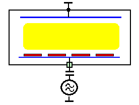 |
* Large anisotropy * Good structure transfer |
* Low selectivity * Low etch rate * Surface damage |
| Anodically coupled plasma etching | 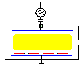 | * High selectivity * High etch rate * Low surface damage |
* Tendency to underetch mask (bad anisotropy) |
| MRIE Magnetically enhanced RIE |
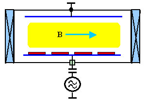 |
* Large anisotropy * High etch rate * Reduced surface damage * Etching relatively independent of loading | * Homogeneity is a problem |
| TRIE Triode reactive ion etching |
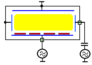 |
* Large anisotropy * Increases process optimization potential with generators |
* Increased costs and complexity |
| TCP Transmission coupled plasma etching or Inductively coupled plasma etching |
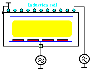 |
* Etching relatively independent of loading * Very large etch rates because of high plasma density | * Constructive problems (no ferromagnetic steels can be used) |
| Well, you get the idea. And if you do not understand exactly how this works (consider the variations in what is grounded and if their is a capacitor), don't worry: It is quite involved. Lets just look at the first two examples: | ||
| Here is RIE, the first example given in the table. | ||
| In the case of pure RIE, the high frequency voltage is coupled capacitively to the lower electrode that carries the wafers. The upper electrode is grounded, and together with the chamber it has a much bigger surface then the lower electrode. | ||
| This will lead to a negative charging of the lower electrode (the reasons for that are tricky and due to the fact that no DC currents can flow, and that the mobility of the negative electrons and positively charged ions is very different). | ||
| The positive ions thus are strongly accelerated before the hit the substrates to be etched; typically they have energies > 100 eV. | ||
| If we keep the pressure low enough, there is hardly any scattering of the ions, and the impinge nearly vertically on the substrates. | ||
| Now lets look at the second case, anodically coupled plasma etching. | ||
| It looks rather similar to the first case, we just changed the connection of the HF generator and the ground. | ||
| This simply reduces the negative charge on the lower electrode, and thus the energy of the ions hitting the substrates. | ||
| In addition, we will keep the pressure rather high, making sure that the ions accelerated in the direction of the substrate have many collision with gas molecules and thus bombard the substrate from all directions. This also reduces their energy, and etching is less "physical" and more "chemical". We gain in selectivity and loose anisotropy. | ||
| But now we will stop. While you should marvel at the complexity of plasma etching, you should not despair. It was people like you - and not the Noble prize winners in physics - who made it work and continue to improve the technique. | ||
© H. Föll (Electronic Materials - Script)