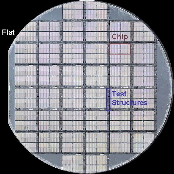
 |
How to get the chips on the wafer? In order to produce a CMOS structure
as shown before, we essentially have to go back and forth between two two basic
process modules: |
 |
Material
module |
|
 |
Deposit some material on the surface of the wafer (e.g. SiO2), or |
|
 |
Modify material already there (e.g. by introducing the desired doping), or |
|
 |
Clean the material present, or |
|
 |
Measure something relative to the material (e.g. its thickness), or |
|
 |
- well, there are a few more points like this but which are not important at this stage. |
 |
Structuring
module |
|
 |
Transfer the desired structure for the relevant material into some light sensitive layer called
a photo-resist or simply resist (which is a very special electronic
material!) by lithography, i.e. by projecting a slide (called a mask
or more generally reticle ) of the structure onto the light sensitive layer, followed by developing
the resist akin to a conventional photographic process, and then: |
|
 |
Transfer the structure from the resist to the material by structure
etching or other techniques. |
 |
Repeat the cycle more than 20
times - and you have a wafer with fully processed chips. |
|
 |
This is shown schematically in the drawing: |
| |
|
|
 |
For the most primitive transistor imaginable, a minimum of 5 lithographic steps are
required. Each process module consists of many individual process steps and it is the
art of process integration to find the optimal combination and sequence of process
steps to achieve the desired result in the most economic way. |
 |
It needs a lot of process steps - most of them difficult and complex - to make
a chip. |
|
 |
Even the most simple 5 mask process requires about 100 process steps.
|
|
 |
A 16 Mbit DRAM needs about 19 masks and 400 process steps. |
 |
To give an idea what this contains, here is a list of the ingredients
for a 16 Mbit DRAM at the time of its introduction to the market (with time it tends to become somewhat simpler): |
|
 |
57 layers are deposited (such as SiO2 (14 times), Si3N4,
Al, ...). |
|
 |
73 etching steps are necessary (54 with "plasma etching", 19 with wet chemistry). |
|
 |
19 lithography steps are required (including deposition of the resist, exposure, and
development). |
|
 |
12 high temperature processes (including several oxidations) are needed. |
|
 |
37 dedicated cleaning steps are built in; wet chemistry occurs 150
times altogether. |
|
 |
158 measurements take place to assure that everything happened as designed. |
 |
A more detailed rendering can
be found in the link. |
 |
Two questions come to mind: |
|
 |
How long does it take to do all this? The answer is: weeks if everything always works and you never have to wait, and months
considering that there is no such thing as an uninterrupted process flow all the time. |
|
 |
How large is the success rate? Well, lets do a back-of-the-envelope
calculation and assume that each process has a success rate of x %. The overall yield
Y of working devices is then
Y = (x/100)N % with N = number of process steps. With N = 450
or 200 we have
|
|
|
| x |
Y for N = 450 |
Y for N = 200 | | 95% |
9,45 · 10–9 % | 3,51 · 10–3 % |
| 99% | 1,09 % | 13,4 % | | 99,9% |
63,7 % | 81,9 % |
|
|
 |
N = 200 might be more realistic, because many steps (especially controls) do not influence
the yield very much. |
 |
But whichever way we look at these numbers, there is an unavoidable conclusion
: Total perfection at each process step is absolutely necessary! |
| |
| |
|
|
|
© H. Föll (Electronic Materials - Script)
