 |
If we look at the cross-section of
the CIGS cell in the preceding subchapter, we see parts of what we are up to if want to mass produce this type of thin film solar cell.
|
|
 |
We have to deposit various thin films on a glass substrate. In order of appearance
we have - Mo
- CIGS
- CdS
- Intrinsic-ZnO
- Al doped ZnO
- Some Polymer
and then put the lid on - another glass plate. |
|
 |
Then we must "put the lid on" - another glass plate. |
 |
The CIGS materials would be the "base" of the solar cell diode
or the principal absorber material; it is always p-doped. The CdS and the i-ZnO form the n-doped
or emitter part of the diode. They have bandgaps different from that of CIGS, so we actually have what is called
a hetero-junction, something we will encounter extensively in Optoelectronics. |
|
 |
Hetero-junctions have basic properties similar to the pn-juntion we know, but a number of peculiarities, too, which we will not go into at present. The CdS
layer, a rather crucial part of the CIGS solar cell, also serves as "buffer"
layer, mediating the lattice mismatch between CIGS and ZnO, a necessary function to keep the interface
properties in the tolerable range. |
|
 |
The heavily p-doped (by Al) top ZnO layer provides the transparent
front side contact (and, perhaps, some anti-reflection coating). |
|
 |
The two top layers of polymer and glass are rather "trivial"; the essentially
keep the rain out and just protect the whole cell for 20 years or so from the environment (including things like
extremely corrosive birds shit). |
 |
The first task thus is to deposit those layers - on a substrate typically 1
m × 1m in size or, using some a role-to-role process, on a flexible substrate like polyimide or stainless steel
that moves inside some piece of equipment at 1 m/min or so and comes out at the other end with at least some of the
relevant layers on it. |
|
 |
For layer deposition we can use some of the processes we learned about earlier, use some that have been around but that we have not encountered yet,
or use the ones especially invented for exactly this task. In other words: We cannot go into this here at all. |
|
 |
Instead we look at some specialities of thin film layer solar cell production
that goes beyond "merely" depositing thin films on a substrate |
| |
|
|
"In-situ" Series Connection |
| | |
 |
As we have seen before,
having very low series resistances is decisive if you want to have a solar cell with an efficiency h
> 10 % or so. |
|
 |
Unfortunately, even heavily doped ZnO - a member of the important material
class of "TCO"
or transparent conductive oxides - has a lousy specific conductivity
of at best 200 µWcm - two orders of magnitude above that of decent metals like Ag
or Cu. |
|
 |
Worse, the intrinsic ZnO layer is almost an insulator, and the CIGS
itself is also not overly conductive. We have a problem shown in the left half of the picture below; the right half shows
the solution. |
| |
 |

Courtesy of Dr. Powalla; ZWS Stuttugart,
© Powalla / ZWS Stuttgart |
|
|
 |
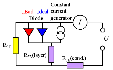
In some simple equivalence circuit diagram we must split the total series resistance
somehow into an internal series resistance coming from the active layers and an "external" one coming from the
"wiring", i.e. the conductors. The bad one is the internal one, because there is not much we can do about that
for a single solar cell. This is one of the reasons why we do not use a low-resistance metal grid like for the Si
bulk solar cell in this case: it wouldn't help much to bring the series resistance down. |
|
 |
The only way to cope is to make the individual solar cells small in one direction (z-direction)-
we have a stripe of about 1 cm in width and up to 100 cm long - and to switch these stripes in series. In
other words, we produce little current in z direction but a lot of voltage. The voltage loss in the internal
resistance is proportional to the current; if we keep the current low, we keep the internal losses down. In other words
we use the same kind of reasoning that leads to high-voltage power lines in the face of finite line resistances. |
|
 |
The problem, of course, is that we cannot manufacture individual stripes of thin film solar
cells and then solder them together - we must do all this series connection "in-situ" while we deposit the various
layers - fast and cheaply. |
 |
Sounds difficult - is difficult. We can also learn an important lesson: |
|
 |
A potential disadvantage - large internal resistances - may be turned into an advantage. Just
solve the problem of how to do "automatic" series connections, and you are no longer producing mediocre solar
cells but large-area solar modules with a high-voltage output that not only alleviates
the internal resistance problem but is just perfect for the power conversion electronics that must come after the module. |
|
 |
As always, there are a few second-order problems with this approach too, but basically it
is a sound approach that is used with practically all thin film solar cells. |
 |
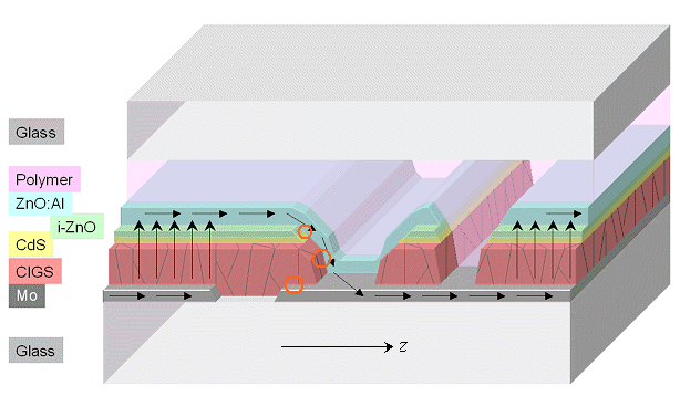
The way it is done is shown in the schematic cross-section of a CIGS solar
cell at the left-hand part of the picture above. If you follow the black arrows symbolizing current flow, you clearly see
that the top of the left cell is connected to the bottom of the right cell; we have a series connection. |
|
 |
If you look at the red circles, you see also that we three nominal short circuits in this
structure:
- The ZnO:Al layer, which is the front side "conductor" here, short circuits the junction formed by the
CIGS and the CdS/i-ZnO.
- The ZnO:Al layer also short circuits to the backside contact via the CIGS layer.
- Both cells are short-circuited at the backside via the Mo layer overlap.
|
|
 |
This doesn't seem to make much sense. However, the short-circuits for the real thing are only
nominal. In reality they have very high resistances (partially because the overlap areas are tiny) and therefore can be
tolerated. If we accept this without further proof, a question still remains: |
|
 |
Why? Why is this connection structure not made in a way that avoids these nominal short circuits?
Even it they don't matter much, wouldn't it be better to stay on the safe side? |
|
 |
The answer is: No! The way its done is the best - all things considered. One could easily
draw cross-sections of smarter structures, but don't forget, you have to make them - cheaply and quickly. This leads to
a little exercise: |
| |
|
 |
By now you should be utterly confused - and that is the point: What we see here
(again) is that the simple issue of making solar cells, very simple devices after all, immediately blows up into your face
and gets rather complicated if you look at any "detail". |
|
 |
We will not go into more details here, but keep in mind that thin film solar cells modules are quite different from bulk Si solar cell modules. |
| | |
|
Building and Running a Thin film Solar Module
Factory |
| |
|
 |
So your laboratory-scale process for a novel thin film solar cell has been very
successful.- you can make something like (5 × 5) cm2 solar cells that have a decent efficiency of
h = 15 % and can be made by what appears to be cheap processes. |
|
 |
All that remains to be done is to built and equip a small (pilot) factory, capable
of producing, let's say, solar cells good for 10 MWp per year. Having in mind that it takes about 8
m2 for 1 kWp; we are talking about 8.000 m2 solar cell area per year,
or 22 m2 per day. You want to process 1 m2 at a time, i.e. make a whole module in one
go. |
|
 |
Where do you buy the layer deposition equipment and whatever else you need? The
companies serving the microelectronic community can't offer anything for that kind of area. Companies making equipment for
flat panel displays are more on target, but they don't know, for example, how to deposit CdS. |
|
 |
And no company out there can help you with what ever it takes to do the in-situ
series connections. |
 |
Your only choice left in the beginning it to make your own equipment, optimally
in cooperation with some company that has a solid background in the general area. |
|
 |
After you did that, and it works, you do what? you keep it to yourself! |
|
 |
Keeping this in mind, you understand why there is so little information around
about how you actually make thin film solar cells on a large scale, and why there are some many variants of any process
discussed in the literature. |
 |
What we are witnessing is an evolutionary process - trial and error - where competition
on any level and survival of the fittest determines the outcome - and this is not necessarily what "pure" science
would have chosen. |
© H. Föll (Semiconductor Technology - Script)