 |
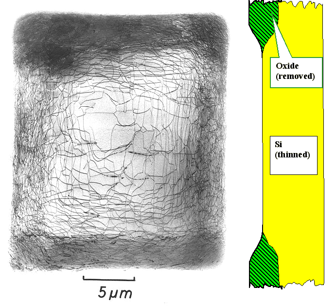
Here is another picture of oxide edge dislocations, this time showing the complete
area of the field oxide |
|
|
|
|
 |
The graphics on the right indicate the cross section through the specimen (the oxide was removed
during preparation). The areas of Si formerly covered by oxide are now so thin that they are totally transparent
to the electron beam - the dislocated areas seem to float in empty space. |
 |
You may wonder how pictures like this are taken. The link leads to a chapter from
the "Defects in Crystals" Hyperscript explaining how transmission
electron microscopy (TEM) can be used to image defects in crystals. |
 |
However it works, this picture is special. In any TEM image, the electron
beam is passed through the specimen, and pictures with good resolution can only be taken if practically all electrons emerge
from the specimen backside with the same energy they had before entering the specimen |
|
 |
We know that electron beams do not travel very far in solids (the electron beam inside your
monitor does not only not get out, after all, but deposits its energy into a rather thin layer of luminescent material);
if they are supposed not to even slow down, the specimen must be very thin - say 0,5 µm at the most for a conventional
TEM with a beam energy of (100 - 150) kV. |
|
 |
This would mean that the specimen must be thinner than the structure it is supposed to contain
- only the surface near parts of it would show. |
|
 |
This problem was overcome around 1976 by using the high-voltage TEM (HVTEM)
of the Max-Planck-Institute for Metal Physics in Stuttgart - a monster that commanded a beam energy of 650 kV which
was enough to look through samples of (2 - 4) µm thickness. The picture shown above (and some of the other ones
in the Hyperscript) were taken with this machine and therefore show the full richness of the defect structures. |
 |
Very few HVTEMs are in use - they are too expensive (the newest on in Stuttgart
costs about 1,5 · 107 DM), so pictures like the one above are rare. |
| |
© H. Föll (Semiconductor Technology - Script)
