 |
Let's have a quick look a factory where semiconductor
technology is used to make a product. Behold the basic law of semiconductor
processing in this context: | |

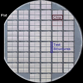
Processed wafer (16 Mbit DRAM; 1990) |
|
| |
| |
| |
Semiconductor Technology
is for making Products
|
| |
| | |
|
 |
Let's pick the most advanced product, a Si microelectronic circuit - a
chip, in other words. |
|
|
 |
There are several factories involved before you get a packaged chip that you
can solder on a circuit board (actually you, personally, would have a hard time doing that, but some machines can). Here
we look at the most expensive and complex part of the production chain: the huge cleanroom
where Si
wafers go in - and Si wafers come out, but now with completed chips on them. |
|
|
 |
The processed wafers as shown in the picture will be turned into packaged chips somewhere
else - often somewhere really else, like 8.000 km away. |
|
|
 |
We can look at the factory as a kind of a (3 · 109€) black box and just look at inputs and outputs. |
|
| |
| |
| |
 |
Severely simplified, here is the basic semiconductor technology plant with its
inputs and outputs: |
|
|
|
 |
Let's look at the boring to annoying factors first: |
|
 |
You need a hell of a lot of money
as input to get going and to keep going. Cost of building and equipping the factory
(some 109€), of developing the product and technology needed, paying the 2.000 - 3.000 people
working there (it's running 24 hours a day, 7 days a week), paying for the input, and paying taxes etc. simply
adds up. You can not reasonably expect the factory to actually sell anything and create money as an output
before 3 years or so are over. |
|
 |
You need to know federal law, state law, local (zoning law), safety regulation, working condition
regulation and so on, and you must strictly comply - otherwise you will be in deep trouble. Are you allowed to do you 24
hours / 7 days shift? Overtime regulations? Safety issues? |
|
 |
Obviously you need people - from lowly operators, via process engineers, team leaders, group
leader to high-up management. You need people able to keep sophisticated equipment running, and you need people able to
buy sophisticated equipment without getting over-charged and running up trouble with tax and custom authorities, and people
able to sell your chips with a profit, if that is possible. The must bring in a lot of know-how, and they take out a lot
of know-how by learning on the job. |
|
| |
 |
Now let's look at the more interesting input. Large groups of extremely knowledgeable
and sophisticated people have defined what the product should be, what kind of performance it should have, and based on
this, came up with the circuit diagrams and it's transformation into a layout, the precise structure in space that this
or that layer is supposed to have on your wafer. | |
 |
| Small part of some lay-out |
|
|
 |
This is encoded into a set of "reticles"
or masks - a kind of slide. one state-of-the art reticle may cost several 10.000 € to make; you need about 20
for a product. So your box full of reticles is not exactly cheap, but the total costs of just making a set of reticles pales
compared to the costs already incurred for coming up with the lay-out. |
|
|
 |
This is essentially the basic product input coming from you colleagues from electrical engineering
and computer science, who have learned how to do this. | |
| | |
| |
 |
Now let's look at the materials input side. |
|
|
 |
Foremost you need Si wafers; several 100 to several 1.000 per day; depending
on the size of your factory and the complexity of your product. If your chip takes 500 processing steps before it
is finished (normal number for normal chips) you cannot process as much per day compared to a more simple chip (e.g. power
chips) needing only 300 process steps. | |
|
 |
We skip the solid materials (the link provides
some examples) and turn to liquids. You need large quantities of simple liquids like water, except that you need it ultrapure
(the factory will have a rather large water processing plant in the basement), and extremely dangerous liquids like (ultrapure)
hydrofluoric acid (HF) as well as other dangerous acids and bases. |
|
|
 |
Then you need a lot of special gases, in particular the most toxic inorganic gases known to
mankind: Arsine (AsH3) and Phosphine (PH3). Other (ultrapure, of course) gases needed
in high volume are merely explosive, e.g. Silane (SiH4) or quite uncommon outside of semiconductor technology
(e.g. WF3). More about that in the link |
|
 |
We will encounter most of these materials when we look at processes, so we will
not go into any more details here. | |
| |
| |
|
 |
On the output side we produce wafers containing fully processed, but not yet measured
and packaged chips. Some of the chips on a wafer may be fully functional, some may be faulty. The percentage of "good"
chips is called the (wafer) yield
h of your factors. It is the most important single number characterizing your factory,
and it should be 100 %, of course. |
|
 |
Haha! When you start to mass produce a new chip generation, you will be lucky
if you make h » 20 %. From then on it's hard work to get it up to 80 %, maybe
90 % over the next few years before your chip is completely outdated anyway. |
 |
In any case, you ship your finished wafers to a place where the get measured (a
pretty complex task). The good ones (after slicing the wafer to separate them) then get packaged (you need another not too
small factory for that - and plenty of know-how and specialized materials) |
|
 |
The they get measured again and, if still working, sold - typically for a few €;
a few chosen ones (microprocessors) for a few 100 € |
|
 |
Do you see the (economic) problem? By the time you sell your first chip of the new generation,
you have already invested a few billion € in its development and production. |
| |
You need to sell one hell of a lot of chips
(at a profit!) to recover your costs! |
|
 |
In other words: Semiconductor technology always
has a money aspect. It just doesn't make much sense to consider it only from a detached and purely scientific point of view. |
© H. Föll (Semiconductor Technology - Script)
