 |
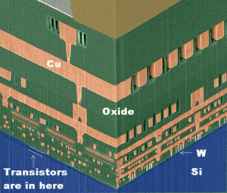
Semiconductor technology is almost synonymous with thin film technology. |
|
|
|
 |
A thin film is always adhering to a substrate and (at least originally) continuous. |
|
|
 |
Thin films may still be found in the product or may have been "sacrificed" during
the making of the product. | |
|
 |
An IC is a study of thin films in and on the Si substrate. |
|
|
 |
The same is true for pretty much every semiconductor product. |
|
| |
| |
| |
 |
Thin always means "thin" relative to some intrinsic (internal) length
scale. Examples are: | |
- Dimensions dx, y, z
- Grain size dgrain
- Lattice constants a0
- l radiation
(light, IR, UV) - Absorption depths
- Mean free path
lengths. - Diffusion length
|
- SCR width dSCR
- Debye length dDebye
- Critical thickness
dcrit
for electrical
break down
- Critical thickness dtu
for tunneling |
|
|
 |
Structural length scales. | |
|
 |
Wavelength and Interaction length scales. | |
|
 |
Transport parameter length scales. | |
|
 |
Electrical scales. | |
| | |
| |
|
 |
There are many thin film applications outside of semiconductor technology: |
| |
|
 |
Optical, electrical, chemical, mechanical, magnetic technologies use thin films. |
| |
| | |
| |
|
 |
Thin films have other spatial properties besides their thickness. |
|
|
|
 |
Interface roughness and surface roughness R defined by their "root
mean square": | |
|
| | |
| |
| |
|
| |
| |
 |
Thin films adhere to their substrate. |
|
|
|
 |
A direct measure of adhesion is the interfacial energy gAB
between film A and substrate B. | |
|
 |
The phase diagram provides some guideline. Complete miscibility=good adhesion, (eutectic))
decomposition=(?) low adhesion. Calculations of g are difficult. |
|
|
 |
Full adhesion can only be obtained for films grown on a substrate. Adhesion energies can be
measured. | |
|
| |
| |
 |
Generally, there will be stress s and strain
e in a thin film and its substrate. | |
Stress and strain in thin films
can be large and problematic!
|
|
|
 |
A major source of strain is the difference of the thermal expansion coefficients a. | |
| | |
|
| |
| eTF |
= |
DT · Da
| | | |
|
| sTF |
= |
Y · DT · Da |
|
| |
| |
| |
| |
 |
Stress in thin film may relax by many mechanisms, and this might be good or bad:
- Cracking or buckling.
- plastic deformation.
- Viscous flow.
- Diffusion.
- Bending of the whole system (Warpage).
| |
|
|
 |
Warpage can be a serious problem in semiconductor technology. |
|
| |
| |
| |
 |
Deposition of a thin layer must start with a "clean" substrate surface
on which the first atomic / molecular layer of the film must nucleate. | |
|
 |
There are many possible interactions between the substrate and "first"
incoming atoms. | |
|
 |
As the interaction energy goes up we move from "some" absorption to
physisorption (secondary bonds are formed) to chemisorption (full bonding) |
|
|
 |
The sticking coefficient is a measure of the likelihood to find an incoming atom in the thin
film forming. | |
|
 |
Immobilization by some bonding is more likely at defects (=more partners). The initial stage
of nucleation is thus very defect sensitive. | |
| | |
| |
 |
Simple surface steps qualify as efficient "defects" for nucleation. |
|
|
|
 |
Small deviations from perfect orientation provide large step densities. Nucleation therefore
can be very sensitive to the precise {hkl} of the surface | |
|
 |
Intersections of (screw) dislocation lines with the surface also provide steps. |
|
|
 |
This may cause grain boundaries and other defects in the growing layer. |
|
|
 |
Scanning probe microscopy gives the experimental background |
|
| |
| |
| |
 |
There is always a nucleation barrier that has to be overcome for the first B-clusters"
to form on A | |
|
|
 |
the three involved interface energies, all expressed in the "wetting angle", plus
possibly some strain are the decisive inputs for the resulting growth mode.
- Frank - van der Merve: Smooth layer-by-layer growth
- Vollmer - Weber: Island growth
- Stranski - Krastonov: Layer plus island growth
| |
| |
| |
| |
| |
 |
Epitaxial layers are crucial for semiconductor technology. |
|
|
|
 |
Misfit of lattice constants will produce strained layers upon epitaxial growth;
strain relief happens by the formation of misfit dislocations. | |
|
 |
Misfit dislocations must be avoided at all costs! |
|
|
 |
Below a usually rather small critical thickness dcrit of the the
thin layer no misfit dislocations will occur. | |
|
 |
Rule of thumb:
0.5 % misfit Þ dcrit
»10 nm | |
|
|
| |
| |
 |
The internal structure of thin films can be anything known from bulk materials
plus some (important!) specialities. | |
a-Si: Micro electronics
a-Si:H: Solar cells, LCD displays
µc-Si:H: Solar cells |
|
| | |
| |
 |
Properties of thin films can be quite different from that of the bulk material. |
|
Much better in thin films
- Electrical break-down field strength of dielectrics.
- Critical current densities in conductors.
|
|
|
 |
The reason can be differences in length scales. |
|
|
 |
Semiconductor technology relies to some extent on superior thin film properties. |
|
|
|
|
© H. Föll (Semiconductor Technology - Script)
