 |
Compounds like InSe, GaSe or Bi2Se3 are called "layered semiconductors" . |
|
 |
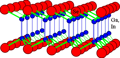
The reason is shown in the picture below. Considering the bonding situation, the two elements
will form two-dimensional layers if the average number of bonds is three (= (4
(Ga, In) + 2 (Se)/2). A GaSe or InSe layer as shown below thus has
no "dangling bonds" and no urgent reason to form a three-dimensional crystal. |
|
 |
Note that there is a certain degree of polytypie with regard to the
arrangement of the layers, but we won't go this deeply into the matter here. |
|
|
 | Structure of III-Se (III = Ga, In, ...)
© prof. Jaegermann, Uni Darmstadt; with permission |
|
 |
A crystal is formed by stacking the layers; the bonding between the layers can only be weak
and of the van-der-Waals (vdW) type |
|
 |
Accordingly, mechanical properties will be extremely non-uniform. It is easy to shear the
crystal in the vdW plane, but not in strongly bonded planes and so on. |
 |
Since the vdW bonded plane has a low density of dangling bonds, but still a perfectly
ordered arrangement of atoms, it is ideal for growing epitaxial
films of other materials. |
|
 |
The atoms of the film to be grown, upon striking the surface of the layered semiconductor
substrate, are not strongly bounded and can move around, but their arrangement will still be influenced by the ordered array
of atoms "below" - and they might follow this order, forming a single crystal. |
|  |
A single-crystal layer growing on a substrate formed by some other crystal usually experiences
increasing strain with increasing thickness because the lattice constants never match perfectly. A relaxation of this misfit
stress is necessary at some critical thickness and misfit
dislocations are commonly introduced. With vdW bonded planes this may not happen - the growing layer "simply"
shears of the substrate, expanding or contracting; whatever is as required to release the stress, because it is only loosely
bound to the substrate. Coherency to the substrate is lost in this case, but that may not be important since the layer can
keep growing to considerable thickness as a single crystal |
 |
As far as semiconducting properties go, here are a few numbers: |
| |
| Type | Lattice | Band Gap | Remarks | | GaSe | hex. |
2-2.1 eV, direct | | | InSe | hex. | 1.2-1.3 eV, direct |
|
|
© H. Föll (Semiconductor Technology - Script)