 |
Making "metallurgical" (= "dirty") Simet
is easy: Þ | |
|
|
 |
A large scale Simet production (> 1 Mio tons/a) exists
for metallurgical ("alloying") and chemical ("silicones") uses |
|
 |
A small amount of Simet (some 20.000 to/a) is purified
(factor 109 or so) to "semiconductor grade Si" Þ |
|
|
 |
Produce high-purity trichlorosilane (SiHCl3) gas in a reactor and distill. |
|
|
 |
Use SiHCl3 and H2 to deposit Si on some Si
core by a CVD process | |
 |
The final result is ultra-high purity (and expensive) poly Si (already
doped if so desired) | |
| | |
| |
 |
Growing a "perfect" single crystal from this poly-Si is not easy
- but possible. | |
|
|
 |
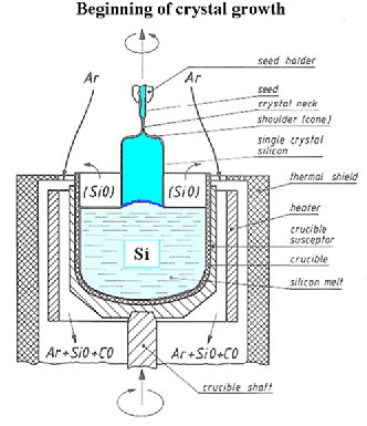
The major crystal growth method is the CZ (= Czrochalski) method: "Pull"
the crystal from a crucible full of molten Si. Þ |
|
|
 |
Some (ususally < 300 mm diameter) crystals are grown by the FZ (= float zone)
method. Somewhat better perfection, but more expensive than CZ. |
|
 |
Major problem: Impurity segregation = general tendency for most impurities (including
doping atoms) to remain (= enrich) in the melt. | |
|
 |
Segregation coeffcient = ccryst/cmelt at interface,
often << 1 and dependent on parameters like growth speed (usually a few mm/min). |
|
|
 |
+ Crystal is purer than melt.
– It is practically impossible to grow a crystal with a uniform impuritiy (including
dopant!) concentration along its length. | |
| | |
| |
 |
Produce wafers by cutting, grinding and polishing |
|
|
|
 |
Extreme precision for a mass product is needed. |
|
|
 |
"Flats" or "notches" (for wafers > 200 mm) identify the crystallographic
orientation and the doping type. | |
|
 |
Beware! Flats are often custome specific and different from the norm. Þ |
|
|
|
| Questionaire |
| Multiple Choice questions to all of 6.1 |
|
© H. Föll (Electronic Materials - Script)

