 |
If Pd instead of Ni is evaporated on a clean Si surface,
hexagonal Pd2Si (a = 0,653 nm, c = 0,344 nm) develops around 200°C
- 300°C. Increasing the annealing temperatures produces no new phases. |
|
 |
The misfit of the hexagonal {001} plane to a Si {111} plane is 1,8%;
we can expect an epitaxial relationship with a misfit dislocation network at a spacing of about 10 nm. This is around
the resolution limit of TEM in a regular contrast mode, so we have to resort to HRTEM and cross-sectional
specimen. |
|
 |
A
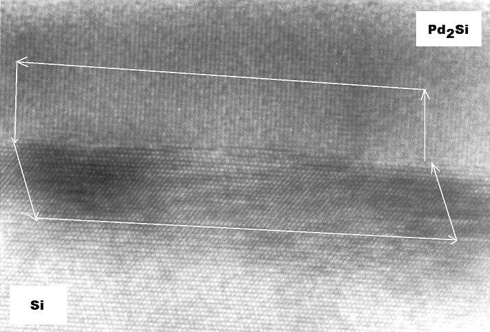
HRTEM image of the interface is shown below (This picture from 1980 is of historical
interest, too: It was, to the best of my knowledge, the first HRTEM picture ever obtained from a phase boundary). |
| |
|
 |
We clearly have an epitaxial layer of Pd2Si. No ending lattice
fringes denoting misfit dislocations are unambigously visible. Therefore a Burgers circuit has been drawn, somewhat analogous to the procedure used to obtain Franks formula. It goes
up in the Pd2Si, then to the left crossing 90 lattice fringes, back to the boundary, 90
fringes to the right and up to the boundary again. It does not close, although it is
clear that it would have closed on a perfectly flat and misfit-dislocation free interface. |
|
 |
Does this mean that the phase boundary contains misfit dislocations? |
|
 |
This is not clear. We may have dislocations in the interface,
but we certainly have steps as can be seen directly. We now have to pay some attention
to the relationship of dislocations and steps, their images in a HRTEM picture,
and their consequences for a Burgers circuit. |
 |
This will lead us into new and quite complicated territory. We will consider the
relationship between steps and dislocations only for the example of hexagonal lattices on cubic lattices, or, more generally,
for S = 3 relations. This will be sufficient to gain an idea of the added complexity. |
© H. Föll (Defects - Script)
