 |
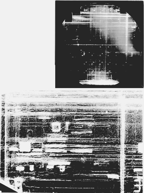
The big advantage of x-ray topography is that it can reveal the defect structure of large samples,
in the case below whole (100 mm) Si wafers. If the negatives are enlarged, details on a 10 µm
scale may be seen. |
| |
|
| |
|

|
X-ray topography of a Si wafer showing "haze"
(milky area in the upper right half) and dislocation structures. The isolated bright small rectangles are transistors full of dislocations
|
 |
Enlargement of an area on the lower left. Some single dislocations are barely
visible; the bright geometric structures correspond to device parts with high densities of dislocations. |
| | |
| |
© H. Föll (Defects - Script)
