 |
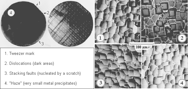
| Shown is a wafer that has been processed to some extent in order to produce integrated circuits. Four kinds of defects were created that can be clearly distinguished, and (with some experience) identified as to their nature and cause of generation. | |||
| |||
| The whole view of the wafer shows the polished front side (left) where not much is visible at this size. The backside (right) has been intentionally roughened by a KOH etch, this accounts for the large scale structure (the intersecting approximate rectangles) in the enlargements in the second half of the picture. | |||
| The four micrographs showing the particular defects can be viewed at higher resolution. Click on the corresponding numbers. | |||
| Picture 1 and 2 | |||
| Picture 3 and 4 | |||
![]() 6.1.1 Observation of Dislocations and Other Defects
6.1.1 Observation of Dislocations and Other Defects
![]() Process-Induced Defects: Large View of Tweezer Marks and Dislocations
Process-Induced Defects: Large View of Tweezer Marks and Dislocations
![]() Process-Induced Defects: Large View of Haze and stacking faults
Process-Induced Defects: Large View of Haze and stacking faults
© H. Föll (Defects - Script)